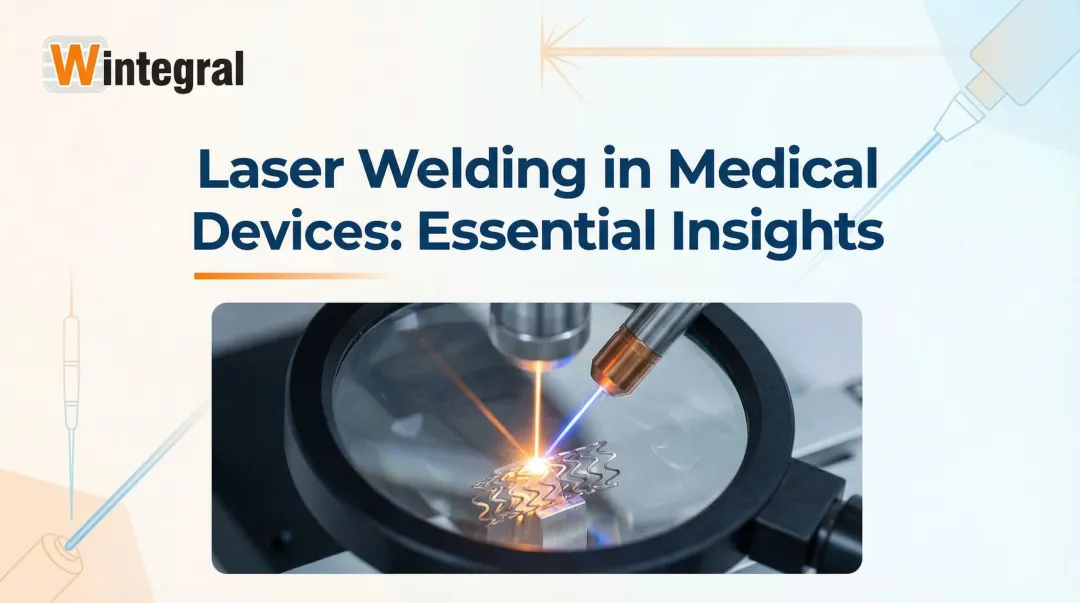
Introduction
When traditional machining methods fail to meet demands for features below 100 μm or tolerances tighter than ±5 μm, manufacturers face costly production delays. Tool and die makers, mould manufacturers, and precision component producers particularly struggle with processing delicate materials without mechanical stress or creating intricate micro-scale geometries.
Laser micromachining is a non-contact material removal technology that uses focused laser beams to create micro-scale features with tolerances as tight as ±1-2.5 μm. Unlike conventional machining, it eliminates tool wear and applies no physical force to workpieces.
The technology minimizes thermal damage through ultrashort pulse technology, making it ideal for heat-sensitive materials and precision repairs.
This article explains the fundamental principles of laser micromachining, explores various techniques from ablation to drilling, and examines industrial applications. Whether you're a manufacturing engineer, tool and die maker, or precision component manufacturer, you'll gain practical insights into when and how to use this advanced processing solution.
Key Takeaways
- Laser micromachining removes material at the micron scale using focused laser energy, achieving dimensional tolerances of ±1-5 μm
- Ultrafast femtosecond lasers enable "cold ablation" with minimal heat-affected zones, producing surface roughness as low as 20-50 nm
- Primary techniques include ablation, drilling (aspect ratios ≥20:1 achievable), cutting, surface texturing, and permanent marking
- Medical devices, semiconductors, aerospace turbine components, and precision tooling repair represent the largest application sectors
- Success requires matching laser parameters to material properties and optimizing scan speed, focal position, and pulse overlap
What Is Laser Micromachining?
Laser micromachining is a precision material removal process using focused laser energy to create features typically between 1-500 micrometers. The technology enables intricate geometries, fine holes, narrow slots, surface patterns, and precise modifications impossible with conventional methods.
How Laser Micromachining Differs from Related Processes
- Macro laser cutting: Operates at larger feature scales (millimeters to centimeters) with looser tolerance requirements
- Laser engraving: Creates surface-only modifications without through-cutting or deep material removal
- Photolithography: Uses masks for pattern transfer rather than direct-write laser processing
These distinctions matter because laser micromachining fills a unique niche requiring both precision and flexibility.
The non-contact nature delivers significant advantages. Without mechanical force, there's no tool wear causing dimensional drift or material deformation from clamping pressure. This enables processing of delicate or brittle materials like thin ceramics and glass.
The Physics Behind the Process
The material absorbs laser light, converting it to thermal or photomechanical energy that causes localized ablation, melting, or vaporization. The specific mechanism depends on laser wavelength, pulse duration, and intensity.
Pulse duration dramatically affects the process. Femtosecond pulses (quadrillionths of a second) remove material before heat can diffuse, while nanosecond pulses create a melt pool that's subsequently ejected.
Why Laser Micromachining Is Used in Precision Manufacturing
The global micromachining market is projected to reach USD $3.3 billion by 2025, growing at 6.2% annually from 2020. This expansion is driven by relentless miniaturization trends and increasingly strict tolerance requirements across multiple industries.
Key adoption drivers include:
- Miniaturization demands: Medical devices have decreased in size by approximately 50% over the past decade, requiring features below 50 μm
- Tighter tolerances: Aerospace navigational systems and engine components now require tolerances of ±5 μm or better
- Complex 3D geometries: Three-dimensional microstructures that traditional 2D methods cannot produce
- Material versatility: Ability to process metals, polymers, ceramics, and composites with a single technology platform
What goes wrong without laser micromachining:
- Mechanical cutting tools break or wear rapidly at micro-scales, causing dimensional drift across production runs
- Chemical etching lacks precision control and generates hazardous waste streams
- Electrical discharge machining (EDM) requires conductive materials and leaves surface defects that compromise part durability
- Traditional methods struggle with feature sizes below 100 μm and cannot achieve the precise depth-to-width ratios needed for modern designs
Quality standards in manufacturing: Modern precision manufacturing demands consistent repeatability and minimal process variation. Laser micromachining's digital process control and inherent accuracy support these requirements, particularly for complex geometries in dies, moulds, and precision tooling where dimensional consistency directly impacts production quality.
The technology has evolved from an R&D novelty to a production necessity. Capability improvements and more affordable laser systems have made micromachining viable for manufacturing environments.
How Laser Micromachining Works (Conceptual Flow)
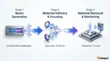
Laser micromachining follows a systematic process built on precision and control. A laser source generates an intense, focused light beam. Beam delivery optics direct and focus this beam to a spot size of 10-50 μm.
Computer-controlled motion systems position the workpiece with micron-level accuracy. The focused energy removes material through ablation, vaporization, or controlled melting.
The process requires three key inputs:
- Workpiece material with specific absorption characteristics at the laser wavelength
- Process parameters including laser power, pulse duration (femtosecond to nanosecond), repetition rate (kHz to MHz), and scan speed
- Assist gas such as compressed air, nitrogen, or argon to remove debris and prevent oxidation
Material transformation mechanism: Photon energy absorption excites electrons in the material. This energy rapidly transfers to the lattice structure, causing the material to reach its ablation threshold.
Material is ejected as vapor, plasma, or particles. The process repeats with each laser pulse, creating layer-by-layer material removal.
Process control systems: Beam positioning via galvanometer scanners or linear stages achieves accuracy to ±1 μm. Positioning accuracy of ±0.5 μm is routinely achieved with computer-controlled XY linear stages.
Modern systems incorporate real-time power monitoring, temperature sensing, and machine vision for alignment and quality verification.
Outcome: Precisely dimensioned features with minimal thermal damage, controlled surface roughness (Ra values of 0.1-1.0 μm achievable), and repeatable results across production runs.
Step 1: Beam Generation and Conditioning
The laser source produces the primary beam with specific wavelength and pulse characteristics. Common wavelengths include:
- UV (343-355 nm): High absorption in most materials, minimal heat-affected zones
- Green (515 nm): Moderate absorption, good for metals and silicon
- Near-IR (1030-1064 nm): Excellent for metals, requires ultrafast pulses for transparent materials
Beam conditioning optics (expanders, attenuators, polarizers) adjust beam properties to match process requirements. Beam quality (M² factor) determines the minimum achievable spot size and therefore the finest features possible.
Step 2: Beam Delivery and Focusing
Once the beam is conditioned, mirrors and lenses direct it to the workpiece. Focusing optics concentrate the energy to achieve the required intensity, often exceeding 10¹² W/cm² for femtosecond pulses. Femtosecond lasers can focus beams to spot sizes as small as 1 μm, enabling extremely fine feature creation.
Focal position relative to the surface determines feature geometry and quality. Focusing slightly above the surface can reduce taper in drilling applications.
Focusing at the surface maximizes material removal efficiency.
Step 3: Material Removal and Process Monitoring
Synchronized motion systems move the beam or workpiece following programmed tool paths. Material is progressively removed either layer-by-layer (for depth control) or in single passes (for through-cutting thin materials).
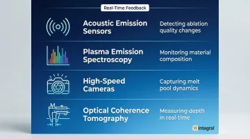
Process monitoring sensors provide real-time feedback:
- Acoustic emission sensors detect changes in ablation quality
- Plasma emission spectroscopy monitors material composition during processing
- High-speed cameras capture melt pool dynamics
- Optical coherence tomography measures depth in real-time
This feedback enables process optimization and quality control, ensuring consistent results across production runs.
Common Laser Micromachining Techniques and Processes
Technique selection depends on the desired feature type, material properties, required precision, and production volume. Each approach offers distinct advantages for specific applications.
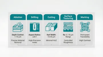
Laser Ablation
Ablation is direct material removal through vaporization, used for creating shallow features, surface texturing, thin film removal, and coating stripping. In silicon, ablation depth increases linearly with pulse energy up to ~15 μm at 150 μJ pulse energy, beyond which plasma shielding reduces efficiency.
Depth control specifications by material:
- Metals: ~1 μm/pulse at 50 J/cm² fluence (nanosecond lasers)
- Glass: 2.0-4.0 mm³/(W·min) removal efficiency (femtosecond lasers)
- Polymers: 0.05-0.5 J/cm² ablation threshold, with optimum processing at 3-10× threshold fluence
Laser Drilling
Laser drilling creates holes from 10 μm to several millimeters diameter using two primary methods:
- Percussion drilling: Stationary beam with multiple pulses drilling straight through
- Trepanning: Circular beam motion creating larger diameter holes with better quality
Aspect ratio capabilities: Advanced femtosecond drilling can produce holes with aspect ratios ≥20:1 in nickel-based superalloys like Inconel 718, maintaining near-zero taper angles (<0.05°). This represents a significant advancement over conventional drilling methods limited to 10:1 ratios.
Key applications:
- Fuel injectors: Holes typically <145 μm diameter for precise fuel atomization
- Medical needles: 50-750 μm diameter holes for drug delivery catheters
- Aerospace cooling holes: 300-500 μm diameter in turbine blades, requiring depth-to-diameter ratios up to 10:1
- PCB microvias: ≥50 μm diameter connection holes in high-density interconnect circuit boards
Tolerances of ±1 μm on hole diameter are achievable in steel with minimised heat-affected zones when using optimised ultrafast laser parameters.
Laser Cutting and Dicing
Continuous or overlapping pulses create through-cuts in thin materials including metals under 1mm, ceramics, and polymers. The technology excels at complex contours and tight inside radii impossible with mechanical sawing.
For semiconductor manufacturing, laser ablation dicing significantly outperforms traditional blade methods:
- Kerf width: 15.4 μm vs. 27 μm (57% narrower)
- Top-side chipping: 2.3 μm vs. 6.2 μm (63% smaller)
- Bottom-side chipping: 13.8 μm vs. 24.3 μm (43% smaller)
- Side wall chipping: Eliminated entirely
Key applications: Stent cutting in Nitinol tubes, microfluidic channel fabrication in glass and polymers, and ultra-thin wafer separation (<50 μm thickness) where mechanical methods cause excessive breakage.
Surface Texturing and Patterning
Controlled laser scanning creates periodic or random surface patterns to modify friction, improve adhesion, or alter wettability properties. Micro-features are typically below 50 μm in scale.
Achievable surface characteristics:
- Roughness range: Ra values from 0.1 μm (smooth) to 8 μm (textured) depending on energy density and scan parameters
- Pattern scales: 100-150 μm diameter dimples with 5-20 μm depth at 30-50% area density effectively enhance hydrodynamic lubrication
- Wettability control: Laser texturing can create superhydrophilic surfaces (contact angle ~0°) or hydrophilic surfaces (<90°) by adjusting the energy density to scanning speed ratio
Applications include cutting tool surfaces for improved chip evacuation, mould surfaces for controlled part release, and medical implants for enhanced osseointegration (bone bonding).
Laser Marking and Engraving
Surface marking creates permanent identification through color change or oxide formation without significant material removal. Engraving removes material to create recessed marks.
Traceability applications include serial numbers, QR codes, and data matrix codes for part tracking throughout the manufacturing lifecycle. Marks are permanent, unaffected by cleaning or sterilisation processes, and machine-readable for automated quality systems.
This capability is essential for medical device compliance with FDA's Unique Device Identification (UDI) requirements.
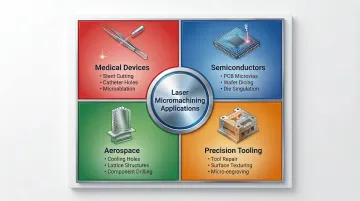
Where Laser Micromachining Is Applied
Primary Application Domains
Medical devices: Surgical instruments require intricate features like serrations and gripping surfaces. Femtosecond lasers cut stents from Nitinol and platinum-iridium tubes with dross-free edges, often eliminating post-processing.
Catheters feature thin struts (29-30 μm) and precise delivery holes (50-200 μm) in multi-lumen designs.
Semiconductor and electronics: UV lasers drill microvias ≥50 μm in high-density interconnect circuit boards, piercing both copper and dielectric layers with high throughput.
For ultra-thin devices (<50 μm), wafer processing relies on laser dicing where mechanical blades cause excessive breakage.
Aerospace components: Turbine blades require thousands of cooling holes (0.3-0.5 mm diameter) with precise angles and positioning. Lightweight structural components benefit from laser-cut lattice structures and precision-drilled fastener holes in advanced alloys.
Precision tooling: High-value moulds and dies benefit from laser micromachining for precision repair work. The technology removes cracks, worn surfaces, and damaged features with minimal material removal.
Service providers like Wintegral Engineering combine laser welding and micromachining for comprehensive mould and die repair, with capabilities ranging from 100-micron micro-deposits to repairs on tools weighing several tonnes.
Lifecycle Positioning
These applications span different stages of a component's life. Laser micromachining occurs during:
- Initial manufacturing: Creating features in new parts during production
- Repair and restoration: Removing damaged material, followed by laser welding restoration and re-machining
- Prototyping: Rapid iteration without tooling investment, with functional microfluidic devices fabricated in under two hours
Typical Implementation Triggers
- New product designs requiring features beyond conventional machining capabilities
- Quality issues with existing processes (burrs, heat damage, dimensional inconsistency)
- Cost reduction initiatives eliminating secondary deburring or finishing operations
- Regulatory requirements demanding validated, traceable manufacturing processes
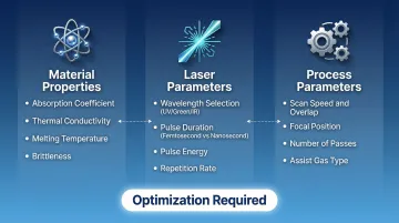
Key Factors That Affect Laser Micromachining Outcomes
Successful laser micromachining depends on the precise interaction of multiple variables. Understanding these factors helps optimize processes for specific materials and applications.
Material properties:
- Absorption coefficient: Determines how efficiently the material absorbs laser energy. Silicon absorbs UV radiation (<380 nm) significantly better than IR
- Thermal conductivity: High conductivity (copper, aluminum) requires higher power or shorter pulses to prevent heat dissipation
- Melting/vaporization temperature: Sets minimum energy thresholds for material removal
- Brittleness: Affects crack formation and edge quality, particularly in ceramics and glass
Laser parameters:
- Wavelength: UV (343-355 nm) for high absorption in most materials and minimal heat-affected zones; IR (1030-1064 nm) for metals with appropriate pulse durations
- Pulse duration: Femtosecond pulses minimize thermal damage and achieve surface roughness as low as 20-50 nm; nanosecond pulses offer higher removal rates at lower cost
- Pulse energy and repetition rate: Control total power delivery and material removal rate. High-power ultrafast lasers (1 kW) achieve removal rates >120 mm³/min
Process parameters:
- Scan speed and overlap percentage: Control surface finish and feature uniformity. Higher overlap (70-90%) produces smoother surfaces with longer processing times
- Focal position: Affects feature geometry, taper angle, and ablation efficiency
- Number of passes: Layer-by-layer removal enables depth control, with each pass removing 1-10 μm depending on material
Environmental conditions:
- Assist gas type and pressure: Nitrogen prevents oxidation in metals; argon protects reactive materials; compressed air suits many general applications
- Ambient temperature and humidity: Affect beam delivery optics and may cause condensation on cooled components
- Vibration isolation: Sub-micron precision requires isolation from building vibrations and acoustic noise
Quality and regulatory requirements:
- Industry-specific standards: Medical devices require biocompatibility testing (ISO 10993); aerospace demands material certifications (AS9100)
- Tolerance specifications: Drive equipment selection and process parameter optimization
- Documentation and traceability: Regulated industries require process validation protocols and batch records for compliance
Common Issues and Misconceptions
Several misconceptions about laser micromachining persist in the industry, often leading to unrealistic expectations or missed opportunities.
"Any laser can do micromachining": Standard CO₂ or fiber lasers used for macro cutting produce excessive heat-affected zones and cannot achieve micron-level precision without specialized focusing optics and ultrashort pulse capability.
The pulse duration matters as much as the wavelength—nanosecond pulses in fused silica produced rough surfaces (Ra 19.97 μm) while femtosecond pulses achieved Ra 1.25 μm.
"Laser micromachining is too slow for production": While single-feature processing takes microseconds to seconds, proper system design enables competitive throughput.
Polygon scanner systems achieve scan speeds up to 800 m/s, processing 7680 cm²/min on stainless steel. Multi-beam processing and optimized scan strategies further increase productivity.
"Results depend only on laser power": Pulse duration, wavelength, focal spot size, and scan strategy are equally or more important than raw power. Increasing pulse energy to boost ablation rates often degrades surface quality. The most efficient strategy maintains optimal fluence while increasing repetition rate.
"Process capability equals process optimization": Having a laser capable of micromachining doesn't guarantee good results without proper parameter development, fixturing design, and quality verification protocols.
Process development typically requires Design of Experiments (DOE) to explore the large parameter space and optimize for specific material-geometry combinations.
When Laser Micromachining May Not Be Appropriate
While laser micromachining offers precision and flexibility, certain applications benefit from alternative manufacturing methods.
Cost-effectiveness considerations:
- Very high volume production: Stamping or molding offers lower per-part cost for simple features in millions of units
- Large-scale material removal: Conventional milling is faster when removing cubic millimeters or more of material
- Capital investment: Industrial-grade ultrafast laser systems start around ₹4 crore, with high-power sources alone exceeding ₹1.6 crore
For low-volume applications or precision repair work, specialized job shop services offer more economical solutions. Companies like Wintegral Engineering provide micro-welding and precision repair services without requiring capital investment in laser systems.
Material constraints:
- Highly reflective materials: Polished copper and gold at IR wavelengths can damage optics or produce inconsistent results, requiring UV wavelengths or surface treatment
- Transparent materials at IR wavelengths: Require UV lasers or ultrafast pulses for nonlinear absorption
- Some composites: Mixed absorption properties create processing challenges with inconsistent material removal
Geometric limitations:
- Very high aspect ratio holes (>20:1): Possible but challenging due to debris evacuation and beam attenuation
- Optical-quality surfaces: May require post-polishing to achieve surface roughness below Ra 0.1 μm
- Three-dimensional features with undercuts: Inaccessible to focused laser beam without multi-axis positioning or part rotation
Laser ablation dicing can be 2-3 times more expensive to operate than blade dicing due to consumables and laser maintenance.
However, the elimination of masks and tooling makes laser micromachining cost-effective for prototyping and small-batch production.
Conclusion
Laser micromachining is a precision material removal technology using focused laser energy to create micro-scale features with tolerances and capabilities beyond traditional methods.
The technology has evolved from research laboratories to production floors, driven by miniaturization demands, regulatory requirements, and the availability of more affordable ultrafast laser systems.
Successful implementation requires understanding how laser-material interaction depends on wavelength, pulse duration, and intensity. Equally important is matching the right technique to your application:
- Ablation, drilling, and cutting for material removal
- Texturing and marking for surface modification
- Parameter optimization based on material properties and environmental conditions
Laser micromachining delivers genuine advantages when conventional methods reach their limits: features below 100 μm, tolerances tighter than ±5 μm, processing of delicate materials, and elimination of tool wear.
However, it's not universally superior. High-volume production of simple features and large-scale material removal often favor traditional methods.
For precision repair and fabrication applications—such as those in tool and die maintenance—laser technologies like those used by Wintegral Engineering demonstrate how micromachining principles translate into practical manufacturing solutions. Making informed decisions requires understanding both capabilities and limitations within your specific manufacturing context.
Frequently Asked Questions
What is the process of micromachining?
Micromachining creates features in the 1-1000 micrometer range using methods like laser micromachining, micro-milling, micro-EDM, and chemical etching. Laser micromachining uses focused laser energy for non-contact material removal, eliminating tool wear and mechanical forces.
What are the common laser micromachining techniques and processes?
Primary techniques include laser ablation (surface removal), laser drilling (high-aspect-ratio holes), laser cutting (through-cuts in thin materials), surface texturing (friction/wettability modification), and laser marking (traceability codes).
What materials can be processed with laser micromachining?
Nearly all engineering materials can be processed: metals (steel, titanium, aluminum), polymers (PEEK, polyimide), ceramics (alumina, zirconia), and composites. Success requires matching laser wavelength to material absorption characteristics.
How does laser micromachining compare to traditional machining methods?
Laser micromachining achieves finer features (down to 1 μm) and tighter tolerances (±1-5 μm) than conventional methods without tool wear or mechanical forces. It excels with heat-sensitive materials but has slower material removal rates and higher capital costs.
What industries benefit most from laser micromachining?
Medical devices (surgical instruments, implants, catheters requiring features below 100 μm), semiconductors and electronics (wafer processing, PCB microvia drilling), aerospace (turbine blade cooling holes, lightweight structures), and precision tooling (mold repair and surface texturing) represent the primary beneficiaries due to their stringent tolerance and miniaturization requirements.
What are the typical tolerances achievable with laser micromachining?
Dimensional tolerances of ±1-5 μm are routinely achievable with optimized ultrashort pulse systems, with positioning accuracy better than ±1 μm. Femtosecond lasers achieve surface roughness as low as 20-50 nm on metals and semiconductors.